Research
![]()
Research projects
Our projects are funded by the DFG via individual projects, the Collaborative Research Center SFB 1277 Emergent Relativistic Effects in Condensed Matter, and the Halle-Berlin-Regensburg Cluster of Excellence Center for Chiral Electronics.
Semiconductor moiré materials with strong spin-orbit coupling
This project investigates the effects of moiré superlattices (Figs. 1a and 1b) in van der Waals homo- and heterobilayers based on semiconducting transition-metal dichalcogenides, specifically MoSe₂, WSe₂, and WS₂. Moiré superlattices arise in these structures due to differences in lattice constants between the constituent layers and/or a nonzero twist angle (Figs. 1a and 2). In selenide-based heterostructures (e.g., MoSe₂/WSe₂), atomic reconstruction occurs in untwisted and small-angle-twisted configurations. In contrast, sulfide-selenide heterobilayers (e.g., MoSe₂/WS₂) exhibit moiré superlattices even without a twist, driven by the larger lattice mismatch. We employ low-frequency resonant Raman spectroscopy (e.g., Fig. 1c), as well as continuous-wave and time-resolved photoluminescence measurements using a streak-camera system.

Fig. 1 | (a) Schematic picture of a twisted MoSe2 homobilayer. The green arrows and the green-shaded area mark the moiré supercell, while the red arrows outline the crystallographic supercell. (b) Hexagonal Brillouin zone of layer 1, with reciprocal basis vectors b1 and b2 of the two twisted layers 1 and 2. g is the reciprocal lattice vector of the moiré superlattice. (c) Low-frequency Raman spectra of a series of twisted MoSe2 homobilayers. The small arrows mark moiré phonons.
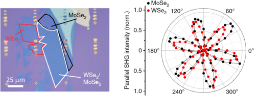
Fig. 2 | Left: Microscope image of MoSe2/WSe2 heterostructure. Right: Polar plot of second-harmonic generation intensities for the determination of the crystal orientations of the constituent layers. A twist angle of about 5° between the MoSe2 and WSe2 layers can be determined.
Ongoing PhD projects:M. Sc. Philipp Parzefall M. Sc. Michael Lorenz |
Van-der-Waals heterostructures with magnetic components
We aim to achieve advanced control over excitons and other electronic quasiparticles in van der Waals heterostructures by integrating additional functional layers. These heterostructures are based on monolayers of semiconducting transition-metal dichalcogenides such as MoSe₂ or WSe₂, combined with functional materials like the layered antiferromagnet CrSBr (Fig. 1a). Time-resolved experiments are conducted using a tunable two-color pump-probe setup, built around a mode-locked Ti:Sapphire laser and a white-light continuum-generating optical fiber. This configuration enables four complementary measurements within a single run: time-resolved Kerr ellipticity (TRKE), transient differential reflectivity (DR), white-light reflectance contrast (RC), and photoluminescence (PL). Emission and absorption properties of quasiparticles are probed via PL (Fig. 1b) and RC (Fig. 1c), while TRKE (Fig. 1d) and DR (Fig. 1e) provide insight into their spin and population dynamics.

(a) Schematic picture of a typical van-der-Waals heterostructure, consisting of monolayer MoSe2, on top of a CrSBr crystal. (b) Photoluminescence, (c) reflectance contrast, (d) time-resolved Kerr ellipticity, and, (e) transient differential reflectivity experiments in the spectral region of the optical bandgap of MoSe2.
Ongoing PhD projects:M. Sc. Andreas Beer M. Sc. Verena Stieß |
Ultrafast magneto spectroscopy of van-der-Waals materials
This project investigates the spin, valley, and pseudospin dynamics in MoSe₂ and WSe₂ multilayers under applied electric and magnetic fields. It builds on our recent discovery of pseudospin quantum beats in these materials, which revealed unexpectedly nonzero in-plane g-factors. To explore the origin of these quantum oscillations in greater detail, we employ time-resolved Faraday ellipticity, transient differential transmission, and time-resolved photoluminescence measurements.
|
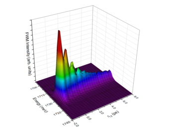
Spectrally-resolved four-wave mixing (FWM) experiment on a GaAs-AlGaAs superlattice, showing coherent Bloch oscillations. |
| Time-resolved Faraday ellipticity experiment on a WSe2 multilayer in an in-plane magnetic field, showing pseudospin quantum beats. An artistic view of the multilayer is projected in the background. | |
Ongoing PhD project:M. Sc. Anna Weindl |
Laboratories of the group
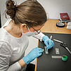
We have five laboratories in our group. One lab for the preparation of 2D crystals and their heterostructures via mechanical exfoliation and deterministic transfer (2D Crystal Fab), and four labs for optical spectroscopy.
2D Crystal Fab
Experiments:
-
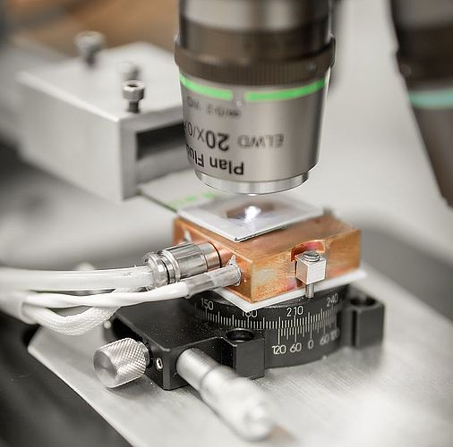
Preparation of single- and few-layer samples via mechanical exfoliation
-
Preparation of artificial hetero- or multi-layer structures via a deterministic transfer process
Pictures:
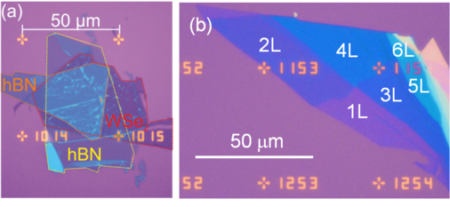
(a) Microscope image of WSe2 layer, encapsulated in hBN layers. (b) Exfoliated MoSe2 sample. The numbers of layers are indicated.

Microscope image of WSe2-MoSe2 heterostructure, prepared by deterministic transfer of single layers.
Ultrafast Spectroscopy Lab I
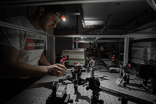
Experiments:
- Time-resolved photoluminescence with streak-camera system
2 ps maximum time-resolution, microscope setup for spatially-resolved experiments, temperatures down to 4 K - Pump-probe spectroscopy, e.g., time-resolved Faraday or Kerr rotation, four-wave mixing, with mode-locked Ti-Sapphire femtosecond laser
Pulse length 100 fs - 600 fs, wavelength range 700 nm - 830 nm, magnetic fields up to 11.5 T, temperatures down to 0.4 K - cw photoluminescence spectroscopy
Spectrometer with 0.5 m focal length and CCD camera, various laser sources, magnetic fields up to 11.5 T, temperatures down to 0.4 K
Ultrafast Spectroscopy Lab II
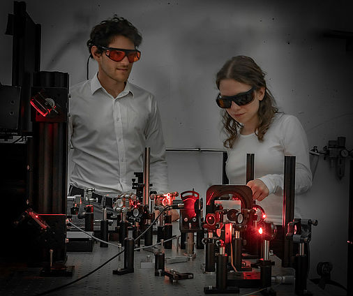
Experiments:
-
Time- and spatially resolved two-color Kerr rotation with mode-locked Ti:Sapphire laser and white-light source
Microscope setup for time- and spatially-resolved experiments, temperatures down to 4 K -
Second-harmonic generation with mode-locked Ti-Sapphire femtosecond laser
Spectrometer with 0.25 m focal length and CCD camera -
Photoluminescence and white-light reflectance
Spectrometer with 0.25 m focal length and CCD camera
Raman Lab I
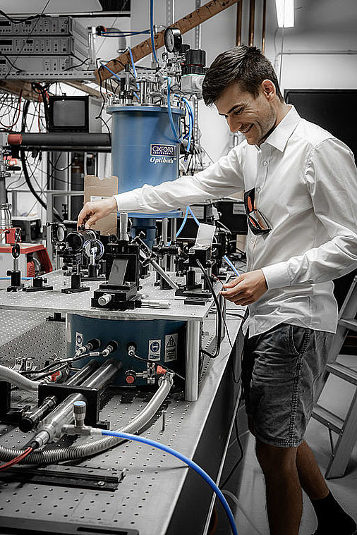
Experiments:
-
Resonant Magneto-Raman Spectroscopy
Triple Raman spectrometer with LN2-cooled CCD detector, tunable cw Ti:Sapphire laser, magnetic fields up to 9 T, temperatures down to 2 K -
Resonant Micro-Raman Spectroscopy
Microscope setup for spatially-resolved experiments, tunable cw Ti:Sapphire laser, temperatures down to 4 K
Raman Lab II
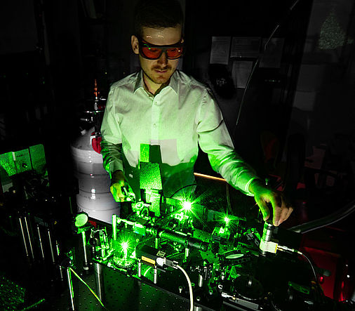
Experiments:
- Micro-Raman Spectroscopy and Mapping
Microscope setup with automated mapping option, spectrometer with 0.5 m focal length and CCD camera, Bragg filter sets for stray-light reduction, various laser sources - White-light reflectance experiments
white-light source, spectrometer with 0.5 m focal length and CCD camera
