We build solid state systems which allow us to experience quantum mechanics and quantization effects in the lab. Our goal is to experimentally uncover the underlying fundamental physics and to develop controllable real-world quantum systems in semiconductors. Possible practical applications encompass scalable quantum bits (qubits) for the implementation of universal quantum computing, sensing schemes based on quantum effects and boosting photonic properties by creating engineered coupling between light and matter.
Experimentally, we study signatures of quantum effects in electronic transport and in luminescence spectroscopy. Many of our quantum systems are realized in specifically designed semiconductor-based nanostructures which we create in molecular beam epitaxy (MBE) crystal growth. Our group has a longstanding expertise in correlating the quantum properties of a system with the crystal properties of nanostructures.
Our current activities cover three research fields:
Spin qubits in gate-defined electronic quantum circuits
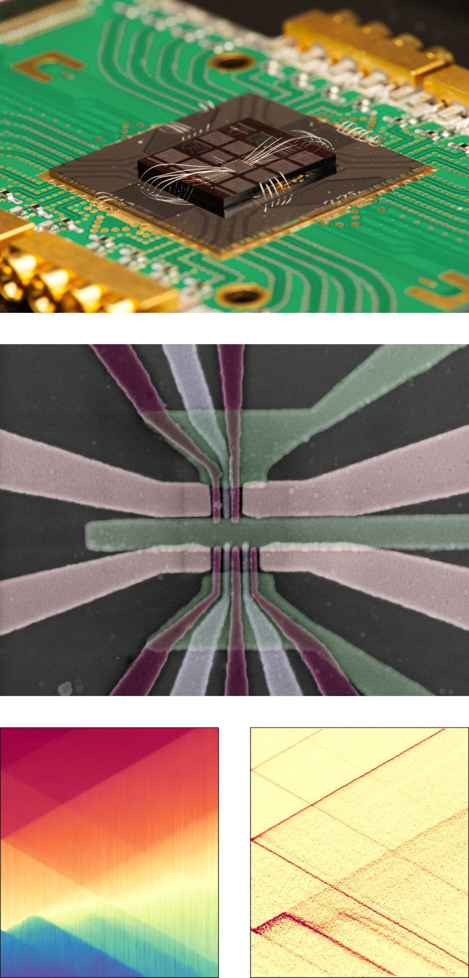
Spin qubits are created via coherent control of single spins in their environment. We build and study chip-based electronic quantum circuits to experimentally implement few-qubit configurations in silicon and in germanium. Low hyperfine interaction in isotope-purified silicon and germanium and limited spin-orbit interaction are key advantages, resulting in attractive spin qubit coherence times. The isolation and the coherent control of single spins are realized in gate-defined Coulomb blockade quantum dot configurations in two-dimensional carrier systems. Our group has a longstanding expertise in gate-controlled rectangular quantum well Si/SiGe (electron spin qubits) and Ge/GeSi (hole spin qubits) semiconductor heterostructures and has pioneered the use of isotope-purified silicon (28Si) and germanium (70Ge) in MBE-grown Si/SiGe and Ge/GeSi heterostructures for spin qubit applications.
Currently, we are particularly interested in uncovering microscopic mechanisms which set the experimental limits of the qubit coherence and different qubit fidelities (initialization, manipulation, readout). Furthermore, we participate in transmitting the knowledge developed in academic labs to industrial pilot-lines, to leverage the synergies with the current silicon chip industry, in order to launch massive upscaling of our comparably small footprint qubit unit cells into chip-based quantum computing processors.
Proximity-induced superconductivity in semiconductors
A superconducting metal placed in the vicinity of a low-dimensional semiconductor carrier system may induce superconductivity into this semiconductor via the proximity effect. Being able to induce superconductivity into a semiconductor carrier systems allows us to explore several new physical phenomena, such as gate-tunable superconducting junctions, unconventional superconductivity in the presence of spin-orbit coupling and the creation of topologically protected eigenstates.
It is anticipated that the interface and the crystalline relationship between the superconductor and the low-dimensional carrier system are of particular importance for the efficiency of proximity-induced superconductivity. Our MBE cluster allows us to grow crystalline thin superconductor films directly – in situ – onto surface-near semiconductor quantum wells. This opens unique possibilities to control the interface and the crystalline relationship between superconductor and semiconductor. We study proximity-induced superconductivity in Ge- as well as in In(Ga)As-based quantum well hybrid heterostructures. One example which we explore is the creation of epitaxial hybrid superconductor/semiconductor heterostructures.
For 2D hole systems in germanium, we develop planar gate-tunable junctions and circuitry elements to realize noise-protected superconducting qubits. For 2D electron systems in the high spin-orbit material In(Ga)As, we explore signatures of unconventional superconductivity and emerging topological state properties.
Nanophotonics and engineered light-matter interaction
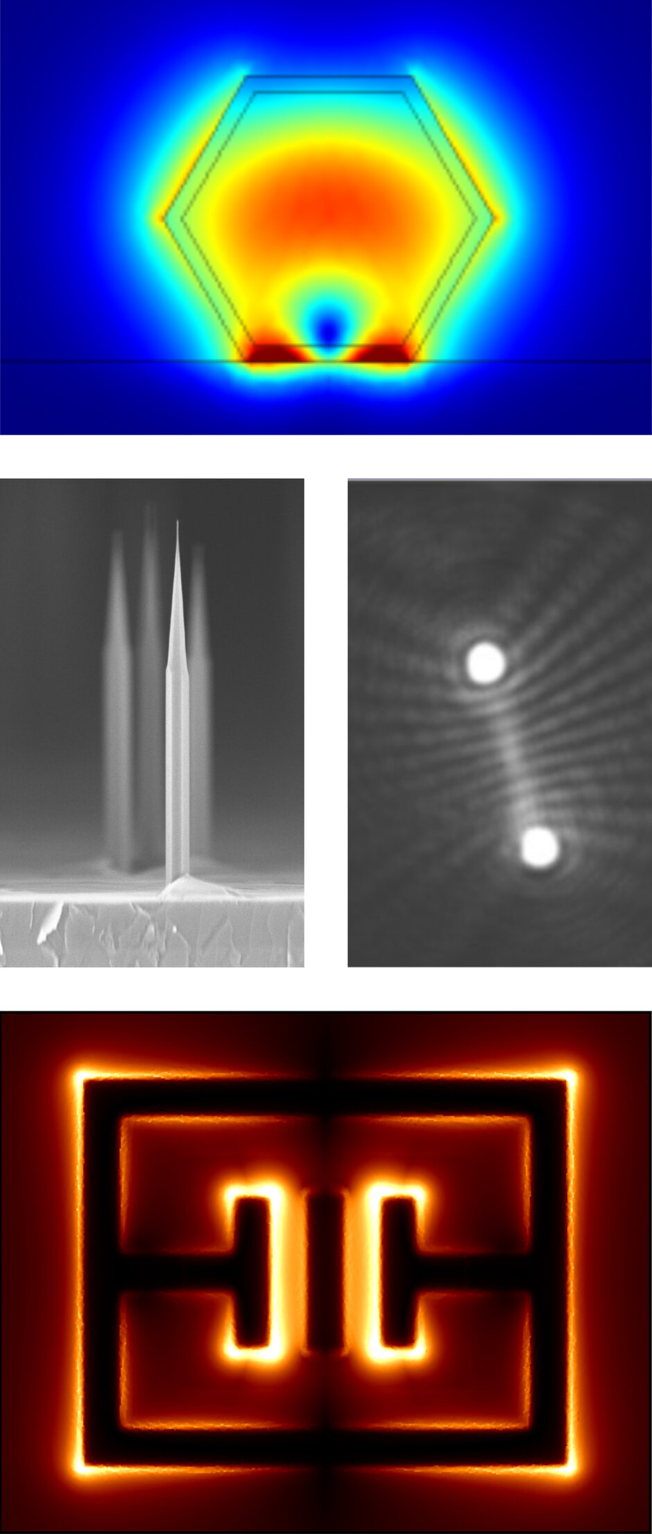
Semiconductor crystals can be excited optically or electrically to spontaneously induce light emission. By engineering the dielectric environment of the excited semiconductor, emitted light can not only be guided into optical modes or trapped in cavities, but also made to strongly interact with the semiconductor, creating phenomena such as stimulated emission.
We build nanocavities and optical mode guiding with custom-tailored dielectric properties, integrated with semiconductor emitters which for example allow us to explore the physics of low threshold lasing and to delve into experimental cavity quantum electrodynamics (cQED).
Regarding low threshold lasing, we are currently experimentally studying the physics governing lasing of single MBE-grown GaAs nanowires, considering aspects such as spatial quantum confinement of the active lasing volume, mode guiding as a function of the nanowire geometry as well as enhanced emission via coupling to engineered plasmonic substrates.
We have realized cQED devices by confining Landau-quantized as well as magneto-plasmonic states in densely packed 2D electron systems with switchable metamaterials. Spin qubits and Josephon junctions also represent quantum mechanical matter systems which can be coupled to superconducting microwave resonators to study cQED.
See also our publications and the thesis titles of our alumni for recent examples of our work:
PhD
| Laura K. Diebel | Si/SiGe spin qubit device building blocks for scalable architectures | 2025 |
| Andreas Schmidbauer | Evaluation of scalable gate architecture components for Si/SiGe spin qubits | 2024 |
| Viola Zeller | Single GaAs nanowire spectroscopy: From 1D quantum confinement to optical waveguiding and lasing | 2023 |
| Michael Prager | Spin-orbit interaction and gate operation in custom-tailored InAlAs-based two-dimensional electron systems | 2022 |
| Thomas Mayer | Epitaxial heterostructures of topological insulators: Band engineering and electronic transport | 2021 |
| Maike Halbhuber | Subcycle dynamics of deep-strong light-matter coupling | 2021 |
| Floyd Schauer | Realizing spin qubits in 28Si/SiGe: heterostructure gating, qubit decoherence and asymmetric charge sensing | 2020 |
| Michaela Trottmann | Characterisation of III-V semiconductor hybrid systems for spinorbitronic functionality | 2020 |
| Florian Dirnberger | New directions for semiconductor nanowires: Demonstrating robust spins and long-lived excitons | 2019 |
| Juliane Laurer | Spininjektion in Silizium | 2018 |
| Andreas Bayer | Ultrastrong THz light-matter interaction in custom-tailored semiconductur heterostructures | 2018 |
| Christian Neumann | Isotopically-enriched 28Si heterostructures for qubit devices | 2017 |
| Josef Loher | Two-dimensional hole systems in indium-based quantum well heterostructures | 2016 |
| Anna Nirschl | Auger-Rekombination und Droop in InGaN Quantentöpfen | 2016 |
| Joachim Hubmann | GaAs nanowires: Epitaxy, crystal structure-related properties and magnetic heterostructures | 2015 |
| Michael Schmalzbauer | Heterostructure design of Si/SiGe two-dimensional electron systems for field-effect devices | 2015 |
| Andreas Wild | Development of a robust platform for spin qubits in SiGe heterostructures | 2013 |
| Martin Utz | Epitaxie von (Ga, Mn)As | 2012 |
| Narayan Sircar | Group IV all-semiconductor spintronics: Materials aspects and optical spin selection rules | 2012 |
| Thomas Zabel | Study on silicon-germanium nanoislands as emitters for a monolithic silicon light source | 2012 |
| Jürgen Sailer | Materials and Devices for quantum information processing in Si/SiGe | 2010 |
| Stefan Ahlers | Magnetic and electrical properties of epitaxial GeMn | 2008 |
Diploma/Master
| Miriam Schweinböck | Signatures of multi-dot configurations in a Si/SiGe SpinBus architecture | 2026 |
| Tobias Biehler | Fabrication and characterization of 2x2 accumulation-mode quantum dot arrays in 28Si/SiGe for spin qubit applications | 2026 |
| Eleonora Buchholz | Observation and investigation of unexpected gate-induced carrier loss in undoped Ge/GeSi quantum well heterostructures | 2026 |
| Matthias Hargasser | Quantum transport in Ge/GeSi: Heterostructure characterization, two-gate-layer quantum dot fabrication and device evaluation | 2025 |
| Leonie Fey | Transverse multimode competition in single GaAs nanowire lasers | 2025 |
| Fabian Tanzer | Fabrication and electrical characterisation of three-gate-layer double dot quantum circuits in Si/SiGe | 2025 |
| Verena Stieß | Few-electron spin qubit device tuning in academic cleanroom and in industrially produced Si/SiGe quantum circuits | 2024 |
| Lukas Zinkl | Biased cooling studies in undoped Si/SiGe field-effect devices for quantum circuits | 2024 |
| Jakob Walsh | Gate operation and magneto-transport characterization of undoped Ge/GeSi heterostructures | 2024 |
| Michaela Zoth | Fabrication and electrical characterisation of quantum circuits for spin qubits in 28Si/SiGe | 2023 |
| Nadine Mundigl | Nanophotonics in single wurtzite GaAs nanowires | 2022 |
| Isabella Knott | Elaboration of a three-gate-layer design for spin qubits in 28Si/SiGe | 2022 |
| Julian Kloiber | Electrostatic gating of topological insulator heterostructures: towards lateral topological p-n junctions | 2022 |
| Lucia Ebnet | Study on spin-orbit coupling in custom-tailored InGaAs/InAlAs heterostructures | 2022 |
| Lukas Herrmann | Photoluminescence spectroscopy of GaAs nanowires in transverse electric fields | 2021 |
| Rudolf Richter | Development and fabrication of a direct accumulation mode qubit device | 2021 |
| Jaydean (Nancy) Schmidt | Controlling the gating behavior in high indium-content heterostructures for spin-orbitronic application | 2021 |
| Florian Schmid | Electronic transport study of band-structure engineered 3D tetradymite topological insulators | 2021 |
| Hedwig Werner | Band structure engineering of 3D topological insulator heterostructures | 2020 |
| Martin Speckner | Designing InAs-based quantum wells for epitaxial superconductor - semiconductor heterostructures | 2020 |
| Carlo Peiffer | Nonlinear charge sensors for Si/SiGe qubit devices | 2020 |
| Wolfgang Himmler | Fabrication and characterisation of Sb-based III/V-semiconductor 2D electron devices | 2019 |
| Andreas Schmidbauer | Electron spin qubits in 28Si: Implementation, single shot readout and spin relaxation times | 2019 |
| Viola Zeller | Ultrastrong light-matter coupling in Landau-quantized electron systems | 2019 |
| Elisabeth Richter | Near-surface InGaAs/GaAs quantum dots: from luminescence properties to coupling to bowtie nanoantennas | 2018 |
| Johannes Baumann | Band structure engineering of the MBE grown topological insulator BSTS | 2018 |
| Thomas Koller | Modulation der spontanen Emission in GaAs-Nanodrähten | 2018 |
| Tobias Weinberger | Magnetotransport characterization of two-dimensional electron systems in undoped silicon quantum wells | 2018 |
| Martin Wieand | Conductance quantization in the high spin-orbit-coupling material InGaAs/InAlAs | 2018 |
| Michael Prager | Realisation of near-surface two-dimensional electron gases in InAs-based quantum wells | 2018 |
| Benjamin Pastötter | Oberflächennahe InAs-basierte Quantenpunkte | 2018 |
| Daniela Krämer | Magnetotransport study of GaAs-based two-dimensional electron systems for efficient field-effect control | 2018 |
| Jan König | Driving GaAs nanowires into the quantum regime | 2017 |
| Simon Schambeck | Optical switching of ultrastrong light-matter coupling | 2017 |
| Helena Doblinger | Elektrische und optische Charakterisierung von Mikrosäulen-LEDs basierend auf dem Materialsystem (Al,Ga,In)N | 2017 |
| Sven Dorsch | Spininjection in Silicon | 2017 |
| Sebastian Schwägerl | Gate-defined Quantum Dots in MBE-grown undoped Si/SiGe heterostructures | 2017 |
| Moritz Forsch | Interface-induced spin-orbit coupling in GaAs core-shell nanowires | 2017 |
| Marcel Pozimski | Ultrastrong light-matter coupling in Landau-quantized systems | 2016 |
| Floyd Schauer | Gate-defined Quantum Dots in undoped Si/SiGe Heterostructures | 2016 |
| Mareen Schäfer | Tunnel structures for spin injection in Silicon | 2016 |
| Christian Fritsch | Elektrostatische Kontrolle von undotierten Si/SiGe-Heterostrukturen | 2015 |
| Florian Dirnberger | Spin Dynamics in Wurtzite GaAs nanowires | 2015 |
| Michaela Trottmann | Spininjektion in Silizium | 2015 |
| Armin Heinrichsdobler | Tunnelstrukturen für Spininjektion in Germanium | 2015 |
| Florian Pickl | Hole-based Quantum Dots in Ge/SiGe Heterostructures | 2015 |
| Tobias Hero | Optische Spektroskopie an dreidimensionalen GaN/InGaN LED-Strukturen | 2014 |
| Juliane Reif | Spininjektion in Silizium | 2014 |
| Sarah Debler | Double quantum dots in a Si/SiGe heterostructure | 2013 |
| Andreas Bayer | Optische Spektroskopie an freistehenden GaAs-Nanodrähten | 2013 |
| Simon Pfaehler | Investigation of undoped Si/Ge heterostructures for double quantum dots | 2013 |
| Christian Neumann | Fabrication and Characterization of Hole Quantum Dots in Ge/SiGe Heterostructures | 2013 |
| Benjamin Esser | Orts- und zeitaufgelöste Spektroskopie an Halbleiternanodrähten | 2013 |
| Patrick Altmann | Spectroscopic characterization of a hybrid structure coupling quantum dots to a two-dimensional electron gas | 2013 |
| Anna Nirschl | Modellierung des elektrischen Transports in blauen InGaN LEDs | 2012 |
| Stefanie Obermeier | Photolumineszenzspektroskopie an niedrigdimensionalen Halbleiterstrukturen | 2012 |
| Michael Schafberger | Electrostatic control of two-dimensional electron gases in Si/SiGe heterostructures | 2012 |
| Ansgar Donner | Gating of hybrid semiconductor nanostructures | 2012 |
| Markus Kargl | Positionskontrolliertes Wachstum von GaAs-Nanodrähten und deren Charakterisierung mit Hilfe von Mikro-Photolumineszenz | 2012 |